
Initial Configuration of STM32H7S78-DK with STM32CubeMX: Bootloader Architecture and XIP Application
Welcome to this technical guide for Learn Embedded Now. In this article, we will cover the complete configuration and startup workflow of the high-performance STM32H7S7L8 microcontroller on the official STMicroelectronics STM32H7S78-DK evaluation board.
The STM32H7R/S family stands out by incorporating an Arm Cortex-M7 core running at 600 MHz alongside an intentionally small internal Flash memory (64 KB). This architectural choice is designed to execute a Primary Bootloader from the internal Flash, which initializes the system and subsequently jumps to the main application. This main application runs directly from a high-speed external Flash memory (XIP - Execute In Place) using XSPI buses.
Throughout this tutorial, we will explore how to configure both contexts (Boot and Application), the external memory manager (ExtMem_Manager), the Memory Protection Unit (MPU), High-Speed Low-Voltage (HSLV) I/O levels, and the External Loader within STM32CubeIDE.
Section 1. Identifying Key Peripherals on the Evaluation Board
Section titled “Section 1. Identifying Key Peripherals on the Evaluation Board”The STM32H7S78-DK development board incorporates two high-speed external memories communicating via the XSPI (Extended Serial Peripheral Interface) hardware subsystem:
- External PSRAM Memory: Uses the XSPI1 peripheral with the Hexa-SPI protocol (16-bit parallel data bus) for dynamic, high-volume data storage at speeds up to 200 MHz.
- External NOR Flash Memory: Uses the XSPI2 peripheral with the Octo-SPI protocol (8-bit data bus) to host the executable code of the main application in XIP mode.
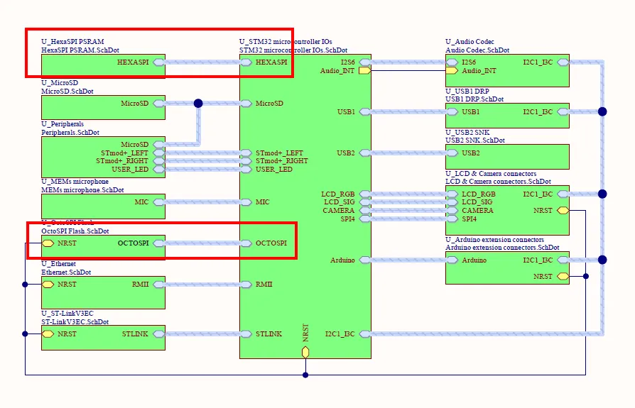
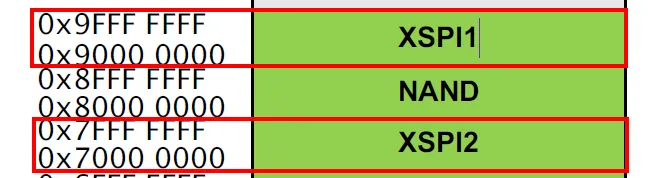
For this project, we will rely on the internal XSPI1 and XSPI2 peripherals. We will configure these in the upcoming sections to achieve both a startup (Boot) and seamless execution of the main program (Application).
Section 2. STM32CubeMX Configuration
Section titled “Section 2. STM32CubeMX Configuration”To visually initialize all the drivers and hardware peripherals, we will use STM32CubeMX. Ensure you match the following environment details to follow along accurately:
- STM32CubeMX Version:
6.18.0 - Firmware Package:
STM32Cube FW_H7RS V1.3.0 - Microcontroller:
STM32H7S7L8H6H
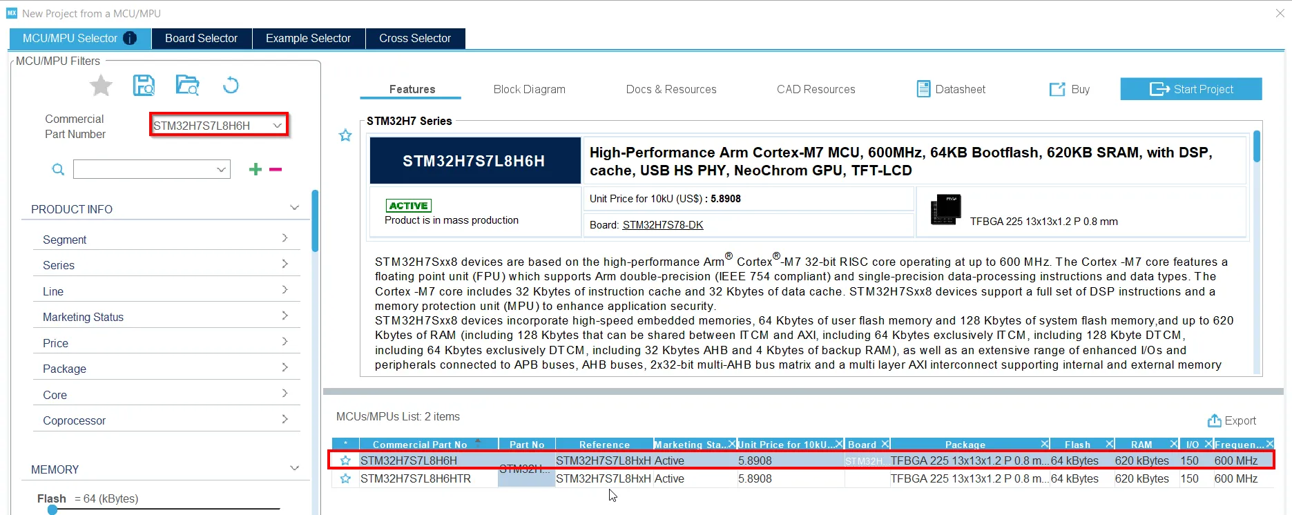
Open STM32CubeMX, search for the exact part number STM32H7S7L8H6H, and start the project as indicated in the image below:
Section 3. XSPI Configuration
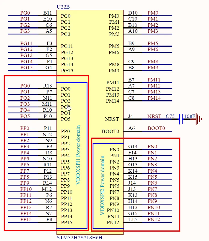
Section titled “Section 3. XSPI Configuration”Properly configuring the XSPI peripheral requires careful consideration of the physical pin layout on the development board. Specifically, the Chip Select Override parameter depends strictly on how the hardware is physically routed in the board’s schematics.
3.1 XSPI1 Configuration for RAM (PSRAM)
Section titled “3.1 XSPI1 Configuration for RAM (PSRAM)”Before diving into the configuration block, it is important to understand our goal here: establishing a high-throughput link to the onboard PSRAM. We select the Hexa-SPI mode to match the physical 16-bit wide bus. The ‘Chip Select Override’ is set to NCS1 - Port1 to ensure the correct chip select pin is driven during memory transactions. We also define the memory size to match our 256 Mbit AP Memory chip, enabling rapid dynamic data access.
Configure the XSPI1 peripheral with the following parameters:
================================================================================XSPI1 CONFIGURATION - STM32CubeMX (STM32H7S7L8HxH)================================================================================
[Device and Context]  - Microcontroller:             STM32H7S7L8HxH  - Peripheral:                  XSPI1  - Runtime Contexts:            Boot (Checked)
[Mode]  - Mode:                        Hexa SPI  - Port:                        Port1 Hexa  - HyperBus(TM) 1.8V Inv. Clock: Disable  - Chip Select Override:        NCS1 - Port1
[Configuration > Parameter Settings]  > Multiplexed:    - Switching Duration Clock Number: 1
  > Generic:    - Fifo Threshold:                  1    - Memory Mode:                     Disable    - Memory Type:                     16BITS AP Memory    - Memory Size:                     256 Mbits    - Chip Select High Time Cycle:     5    - Free Running Clock:              Disable    - Clock Mode:                      High    - Wrap Size:                       32 Bytes    - Clock Prescaler:                 0    - Sample Shifting:                 None    - Chip Select Boundary:            16 KBytes    - Maximum Transfer:                0    - Refresh Rate:                    400    - Memory Select:                   NCS1================================================================================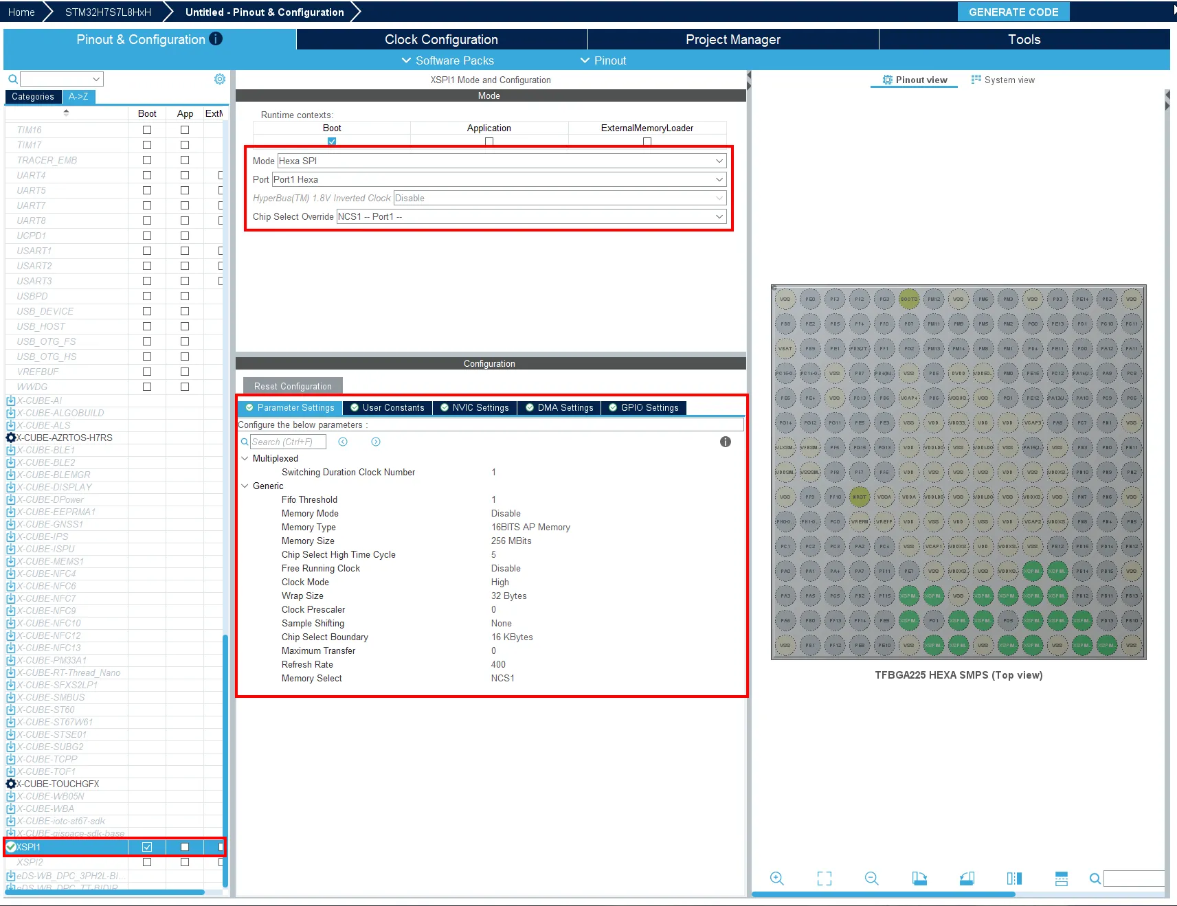
3.2 XSPI2 Configuration for Flash Memory
Section titled “3.2 XSPI2 Configuration for Flash Memory”The NOR Flash memory will host our actual application code. Therefore, XSPI2 is configured in Octo-SPI mode to interface with the 8-bit bus of the Macronix chip. Notice that we assign this peripheral exclusively to the Boot runtime context. This is because the internal Bootloader assumes the responsibility of initializing this bus so that by the time the system jumps to the application space, the memory is already memory-mapped and ready for Execute In Place (XIP).
Configure the XSPI2 peripheral with the following parameters:
================================================================================XSPI2 CONFIGURATION - STM32CubeMX (STM32H7S7L8HxH)================================================================================
[Device and Context]  - Microcontroller:             STM32H7S7L8HxH  - Peripheral:                  XSPI2  - Runtime Contexts:            Boot (Checked) / Application (Unchecked) / ExternalMemoryLoader (Unchecked)
[Mode]  - Mode:                        Octo SPI  - Port:                        Port2 Octo  - HyperBus(TM) 1.8V Inv. Clock: Disable  - Chip Select Override:        NCS1 - Port2 -
[Configuration > Parameter Settings]  > Generic:    - Fifo Threshold:                  1    - Memory Mode:                     Disable    - Memory Type:                     Macronix    - Memory Size:                     1 GBits    - Chip Select High Time Cycle:     2    - Free Running Clock:              Disable    - Clock Mode:                      Low    - Wrap Size:                       Not Supported    - Clock Prescaler:                 0    - Sample Shifting:                 None    - Chip Select Boundary:            Disabled    - Maximum Transfer:                0    - Refresh Rate:                    0    - Memory Select:                   NCS1================================================================================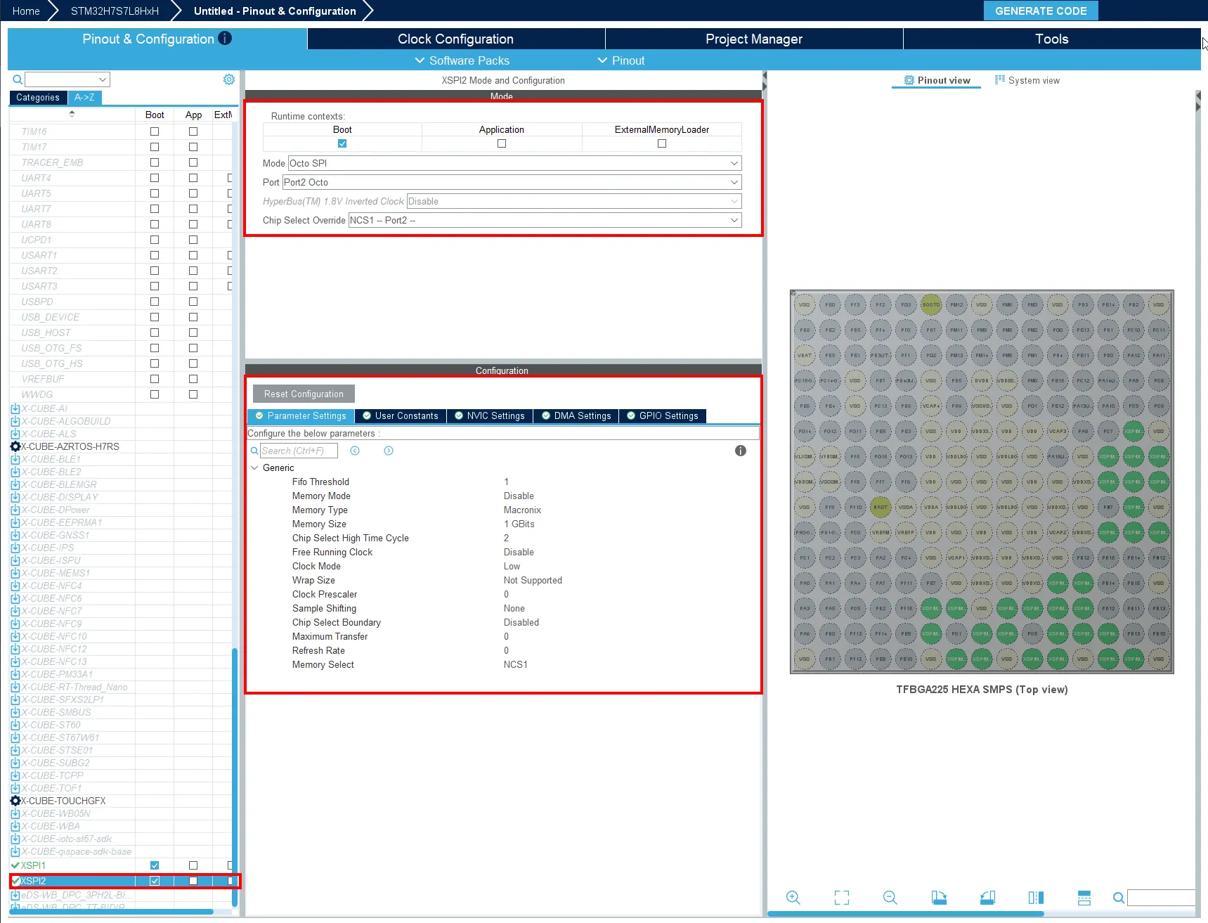
Section 4. RCC and Power Configuration
Section titled “Section 4. RCC and Power Configuration”Power and clock management are foundational for pushing the Cortex-M7 core to its 600 MHz performance limit. In this section, we select the main clock source and configure the internal power supply scheme.
For the official evaluation board, we utilize an external Crystal/Ceramic Resonator to ensure high precision. Additionally, we leverage the internal Switched-Mode Power Supply (SMPS) configured as PWR_DIRECT_SMPS_SUPPLY. This highly efficient step-down converter is implemented by hardware out-of-the-box on this board and provides optimal power regulation for high-frequency operations.
================================================================================RCC CONFIGURATION - STM32CubeMX================================================================================
[Device and Context]  - Peripheral:                         RCC  - Runtime contexts:                   Boot (Checked)                                        Application (Checked)                                        ExternalMemoryLoader (Unchecked)
[Mode]  - High Speed Clock (HSE):             Crystal/Ceramic Resonator  - Low Speed Clock (LSE):              Disable  - Master Clock Output 1:              Unchecked (Disabled)  - Master Clock Output 2:              Unchecked (Disabled)  - Audio Clock Input (I2S_CKIN):       Unchecked (Disabled)  - Digital Clock Input (ETH_RMII_REF): Unchecked (Disabled)  - Digital Clock Input (ETH_CLK):      Unchecked (Disabled)  - CRS SYNC:                           Disable
[Configuration > Parameter Settings]  > Power Parameters:    - SupplySource:                     PWR_DIRECT_SMPS_SUPPLY    - Power Regulator Voltage Scale:    Power Regulator Voltage Scale 0
  > RCC Parameters:    - TIM Prescaler Selection:          Disabled    - HSE Startup Timout Value (ms):    100    - LSE Startup Timout Value (ms):    5000    - HSI Calibration Value:            64
  > System Parameters:    - VDD voltage (V):                  3.3 V    - Flash Latency(WS):                7 WS (8 CPU cycle)
  > PLL range Parameters:    - PLL1 input frequency range:       Between 8 and 16 MHz    - PLL2 input frequency range:       Between 8 and 16 MHz    - PLL1 clock Output range:          High VCO range    - PLL2 clock Output range:          High VCO range================================================================================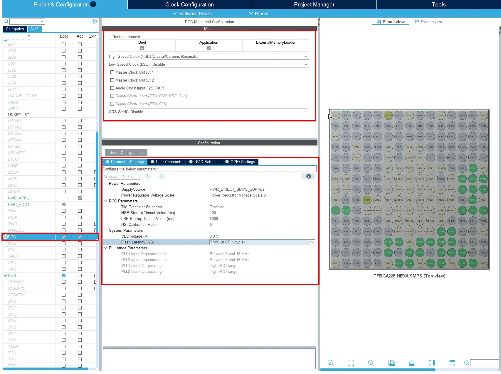
Section 5. SBS Configuration (High Speed Low Voltage)
Section titled “Section 5. SBS Configuration (High Speed Low Voltage)”To achieve the maximum operating frequency on the XSPI lines (up to 200 MHz), the designated I/O pads must operate in HSLV (High Speed Low Voltage) mode. This reduces signal switching times and maintains signal integrity at ultra-high speeds.
Making this mode fully operational requires two distinct steps: the first is declaring it in STM32CubeMX, and the second involves permanently programming the Option Bytes via STM32CubeProgrammer.
5.1 SBS Configuration in STM32CubeMX
Section titled “5.1 SBS Configuration in STM32CubeMX”Enable the HSLV feature for both XSPI ports to ensure the firmware drivers configure the pads accordingly during initialization.
================================================================================SBS CONFIGURATION - STM32CubeMX================================================================================
[Device and Context]  - Peripheral:                         SBS  - Runtime contexts:                   Boot (Checked)                                        Application (Unchecked)                                        ExternalMemoryLoader (Unchecked)
[Mode]  - Activated:                          Checked (Enabled)
[Configuration > Parameter Settings]  > Basic parameters:    - IO HSLV FOR XSPIM1:               ENABLE    - IO HSLV FOR XSPIM2:               ENABLE    - IO HSLV FOR OTHER IO:             DISABLE================================================================================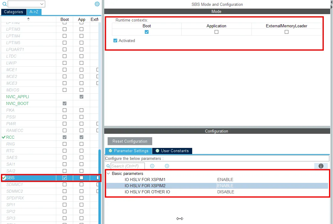
5.2 Option Bytes Configuration in STM32CubeProgrammer
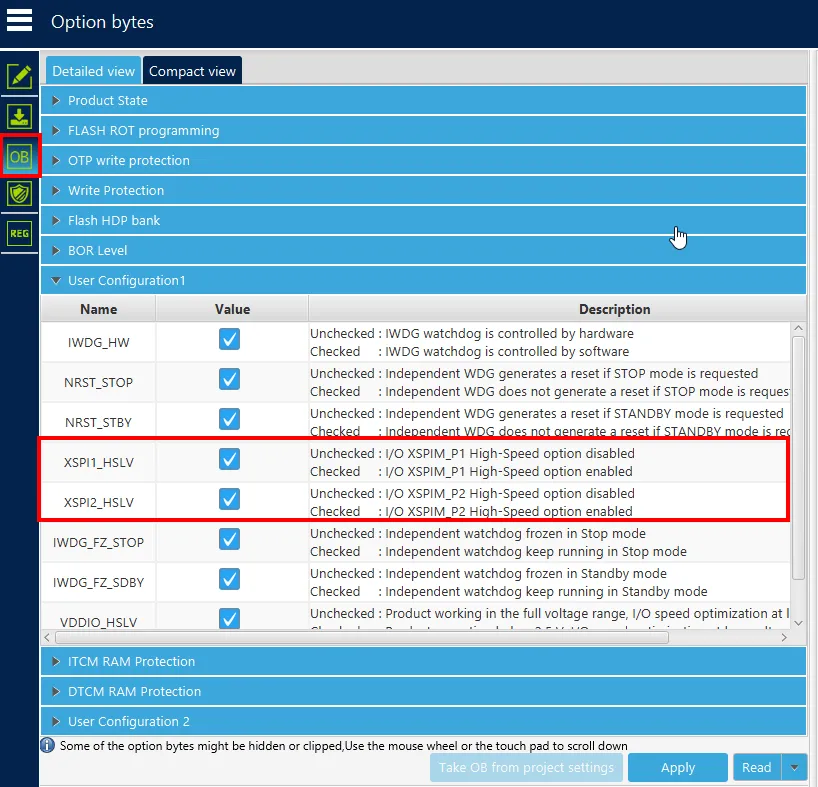
Section titled “5.2 Option Bytes Configuration in STM32CubeProgrammer”The hardware must know about the 1.8V domain immediately upon power-up, before the application code even runs. This is why we must set the option bytes.
- Open STM32CubeProgrammer and connect to your microcontroller via ST-LINK.
- Navigate to the Option bytes section (the OB icon on the left menu).
- Expand the User configuration 1 tab.
- Check the
XSP1_HSLVandXSPI2_HSLVboxes. - Click Apply to write these configuration bits into non-volatile memory.
Section 6. ExtMem_Manager Configuration
Section titled “Section 6. ExtMem_Manager Configuration”The ExtMem_Manager middleware component automatically handles the complex initialization sequences of the external memory buses and configures the Execute In Place (XIP) mapping. This abstracts away the low-level memory controller commands.
6.1 Boot Usecase Configuration
Section titled “6.1 Boot Usecase Configuration”Here, we declare that our primary Boot code will be generated and that the fundamental strategy is to initialize the system and transition into an XIP state, specifically targeting Memory 1.
================================================================================EXTMEM_MANAGER CONFIGURATION (Boot usecase) - STM32CubeMX================================================================================
[Device and Context]  - Peripheral:                         EXTMEM_MANAGER  - Runtime contexts:                   Boot (Checked)                                        Application (Unchecked)                                        ExternalMemoryLoader (Checked)
[Mode]  - Activate External Memory Manager:   Checked (Enabled)
[Configuration > Boot usecase]  > Boot:    - Select boot code generation:      Checked (Enabled)    - Selection of the boot system:     Execute In Place
  > XIP:    - select the memory:                Memory 1================================================================================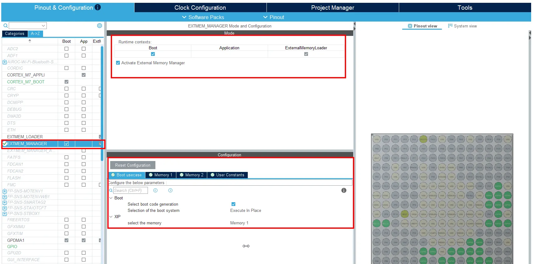
6.2 Memory 1 Configuration (NOR Flash)
Section titled “6.2 Memory 1 Configuration (NOR Flash)”We associate Memory 1 with the EXTMEM_NOR_SFDP driver and link it to the previously configured XSPI2 instance. The SFDP (Serial Flash Discoverable Parameters) driver allows the microcontroller to query the memory chip for its specific capabilities automatically.
================================================================================EXTMEM_MANAGER CONFIGURATION (Memory 1) - STM32CubeMX================================================================================
[Device and Context]  - Peripheral:                         EXTMEM_MANAGER  - Runtime contexts:                   Boot (Checked)                                        Application (Unchecked)                                        ExternalMemoryLoader (Checked)
[Mode]  - Activate External Memory Manager:   Checked (Enabled)
[Configuration > Memory 1]  > Select driver:    - Select the memory driver:         EXTMEM_NOR_SFDP
  > Configuration:    - Memory Instance:                  XSPI2    - Number of memory data lines:      EXTMEM_LINK_CONFIG_8LINES================================================================================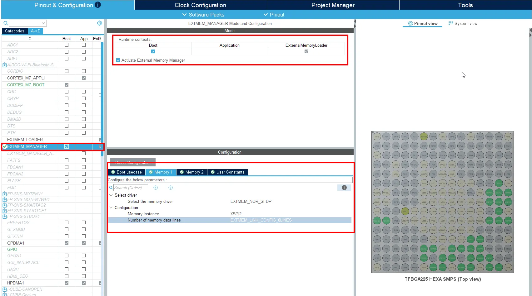
6.3 Memory 2 Configuration (PSRAM)
Section titled “6.3 Memory 2 Configuration (PSRAM)”For Memory 2, we define the low-level command set required to communicate with the PSRAM chip over XSPI1. Since PSRAM doesn’t typically support standardized SFDP discovery like NOR Flash, we must manually input the specific Read/Write commands, register sizes, and dummy cycles derived from the memory chip’s datasheet.
================================================================================EXTMEM_MANAGER CONFIGURATION (Memory 2) - STM32CubeMX================================================================================
[Device and Context]  - Peripheral:                         EXTMEM_MANAGER  - Runtime contexts:                   Boot (Checked)                                        Application (Unchecked)                                        ExternalMemoryLoader (Checked)
[Mode]  - Activate External Memory Manager:   Checked (Enabled)
[Configuration > Memory 2]  > Select driver:    - Select the memory driver:         EXTMEM_PSRAM
  > Configuration:    - Memory Instance:                  XSPI1    - Number of memory data lines:      EXTMEM_LINK_CONFIG_16LINES
  > Memory Info:    - Memory Size:                      HAL_XSPI_SIZE_256MB    - Memory Maximun Frequency:         200 Mhz
  > Memory Command:    - Read Register command:            0x40    - Write Register command:           0xC0    - Register Size:                    2    - Register Dummy Cycles:            4    - Write Command:                    0xA0    - Write Dummy Cycles:               4    - Read Command:                     0x20    - Wrap Read Command:                0x00    - Read Dummy Cycles:                4
  > Memory Configuration:    - Number of Configuration Steps:    1
  > Configuration 1:    - Write Mask:                       0x40    - Write Value:                      0x40    - Register Address:                 0x08================================================================================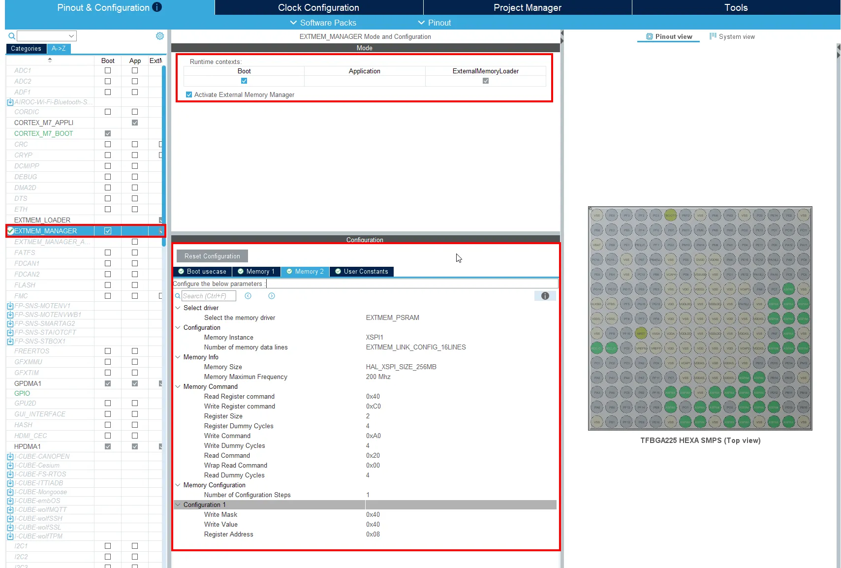
Section 7. Cortex-M7 Boot Configuration (CORTEX_M7_BOOT)
Section titled “Section 7. Cortex-M7 Boot Configuration (CORTEX_M7_BOOT)”Because this microcontroller features a powerful MPU (Memory Protection Unit) and aggressive speculative execution on the Cortex-M7, memory sections must be strictly configured for both the Boot and Application components. Without the MPU, the processor might prefetch instructions from uninitialized memory ranges, immediately throwing a Hard Fault.
To assign these regions correctly, we must map them directly to the base addresses defined by the hardware architecture:
For the startup context (CORTEX_M7_BOOT), our strategy is simple. We create a background region (Region 0) covering the entire 4GB space that explicitly denies all access. This acts as our safety net. Then, we configure Region 1 pointing to 0x70000000 (the XSPI2 base address) to permit data access and instruction execution, enabling a safe jump to the external Flash.
================================================================================CORTEX_M7_BOOT CONFIGURATION - STM32CubeMX================================================================================
[Device and Context]  - Peripheral:                         CORTEX_M7_BOOT  - Runtime contexts:                   Boot (Checked)                                        Application (Unchecked)                                        ExternalMemoryLoader (Unchecked)
[Configuration > Parameter Settings]  > Speculation default mode Settings:    - Speculation default mode:                 Disabled
  > Cortex Interface Settings:    - CPU ICache:                               Enabled    - CPU DCache:                               Enabled
  > Cortex Memory Protection Unit Control Settings:    - MPU Control Mode:                         Background Region Privileged accesses only + MPU Disabled d...
  > Cortex Memory Protection Unit Region 0 Settings:    - MPU Region:                               Enabled    - MPU Region Base Address:                  0x0    - MPU Region Size:                          4GB    - MPU SubRegion Disable:                    0x87    - MPU TEX field level:                      level 0    - MPU Access Permission:                    ALL ACCESS NOT PERMITTED    - MPU Instruction Access:                   DISABLE    - MPU Shareability Permission:              DISABLE    - MPU Cacheable Permission:                 DISABLE    - MPU Bufferable Permission:                DISABLE
  > Cortex Memory Protection Unit Region 1 Settings:    - MPU Region:                               Enabled    - MPU Region Base Address:                  0x70000000    - MPU Region Size:                          128MB    - MPU SubRegion Disable:                    0x0    - MPU TEX field level:                      level 1    - MPU Access Permission:                    ALL ACCESS PERMITTED    - MPU Instruction Access:                   ENABLE    - MPU Shareability Permission:              DISABLE    - MPU Cacheable Permission:                 ENABLE    - MPU Bufferable Permission:                ENABLE================================================================================
Section 8. Cortex-M7 App Configuration (CORTEX_M7_APPLI)
Section titled “Section 8. Cortex-M7 App Configuration (CORTEX_M7_APPLI)”Once the system hands over control to the main program, the application requires broader access to execute user code and manipulate memory safely.
In this Application context configuration, we expand upon the Boot MPU setup. Alongside Region 0 (Global Deny) and Region 1 (Execute Flash), we define additional regions. For example, Region 5 designates the internal RAM block at 0x24000000 to be cacheable and shareable. This carefully tailored setup ensures optimal performance while maintaining strict boundaries for variables and peripherals, which is critical in this tier of microcontrollers.
================================================================================CORTEX_M7_APPLI CONFIGURATION - STM32CubeMX================================================================================
[Device and Context]  - Peripheral:                         CORTEX_M7_APPLI  - Runtime contexts:                   Boot (Unchecked)                                        Application (Checked)                                        ExternalMemoryLoader (Unchecked)
[Configuration > Parameter Settings]  > Speculation default mode Settings:    - Speculation default mode:                 Disabled
  > Cortex Interface Settings:    - CPU ICache:                               Enabled    - CPU DCache:                               Enabled
  > Cortex Memory Protection Unit Control Settings:    - MPU Control Mode:                         Background Region Privileged accesses only + MPU Disabled...
  > Cortex Memory Protection Unit Region 0 Settings:    - MPU Region:                               Enabled    - MPU Region Base Address:                  0x0    - MPU Region Size:                          4GB    - MPU SubRegion Disable:                    0x87    - MPU TEX field level:                      level 0    - MPU Access Permission:                    ALL ACCESS NOT PERMITTED    - MPU Instruction Access:                   DISABLE    - MPU Shareability Permission:              DISABLE    - MPU Cacheable Permission:                 DISABLE    - MPU Bufferable Permission:                DISABLE
  > Cortex Memory Protection Unit Region 1 Settings:    - MPU Region:                               Enabled    - MPU Region Base Address:                  0x70000000    - MPU Region Size:                          128MB    - MPU SubRegion Disable:                    0x0    - MPU TEX field level:                      level 1    - MPU Access Permission:                    ALL ACCESS PERMITTED    - MPU Instruction Access:                   DISABLE    - MPU Shareability Permission:              DISABLE    - MPU Cacheable Permission:                 ENABLE    - MPU Bufferable Permission:                ENABLE
  > Cortex Memory Protection Unit Region 2 Settings:    - MPU Region:                               Enabled    - MPU Region Base Address:                  0x70000000    - MPU Region Size:                          2MB    - MPU SubRegion Disable:                    0x0    - MPU TEX field level:                      level 1    - MPU Access Permission:                    ALL ACCESS PERMITTED    - MPU Instruction Access:                   ENABLE    - MPU Shareability Permission:              DISABLE    - MPU Cacheable Permission:                 ENABLE    - MPU Bufferable Permission:                ENABLE
  > Cortex Memory Protection Unit Region 3 Settings:    - MPU Region:                               Enabled    - MPU Region Base Address:                  0x90000000    - MPU Region Size:                          32MB    - MPU SubRegion Disable:                    0x0    - MPU TEX field level:                      level 1    - MPU Access Permission:                    ALL ACCESS PERMITTED    - MPU Instruction Access:                   DISABLE    - MPU Shareability Permission:              DISABLE    - MPU Cacheable Permission:                 DISABLE    - MPU Bufferable Permission:                DISABLE
  > Cortex Memory Protection Unit Region 4 Settings:    - MPU Region:                               Enabled    - MPU Region Base Address:                  0x20000000    - MPU Region Size:                          64KB    - MPU SubRegion Disable:                    0x0    - MPU TEX field level:                      level 1    - MPU Access Permission:                    ALL ACCESS PERMITTED    - MPU Instruction Access:                   DISABLE    - MPU Shareability Permission:              DISABLE    - MPU Cacheable Permission:                 DISABLE    - MPU Bufferable Permission:                DISABLE
  > Cortex Memory Protection Unit Region 5 Settings:    - MPU Region:                               Enabled    - MPU Region Base Address:                  0x24000000    - MPU Region Size:                          512KB    - MPU SubRegion Disable:                    0x0    - MPU TEX field level:                      level 1    - MPU Access Permission:                    ALL ACCESS PERMITTED    - MPU Instruction Access:                   DISABLE    - MPU Shareability Permission:              ENABLE    - MPU Cacheable Permission:                 ENABLE    - MPU Bufferable Permission:                DISABLE================================================================================
Section 9. Clock Generation Configuration
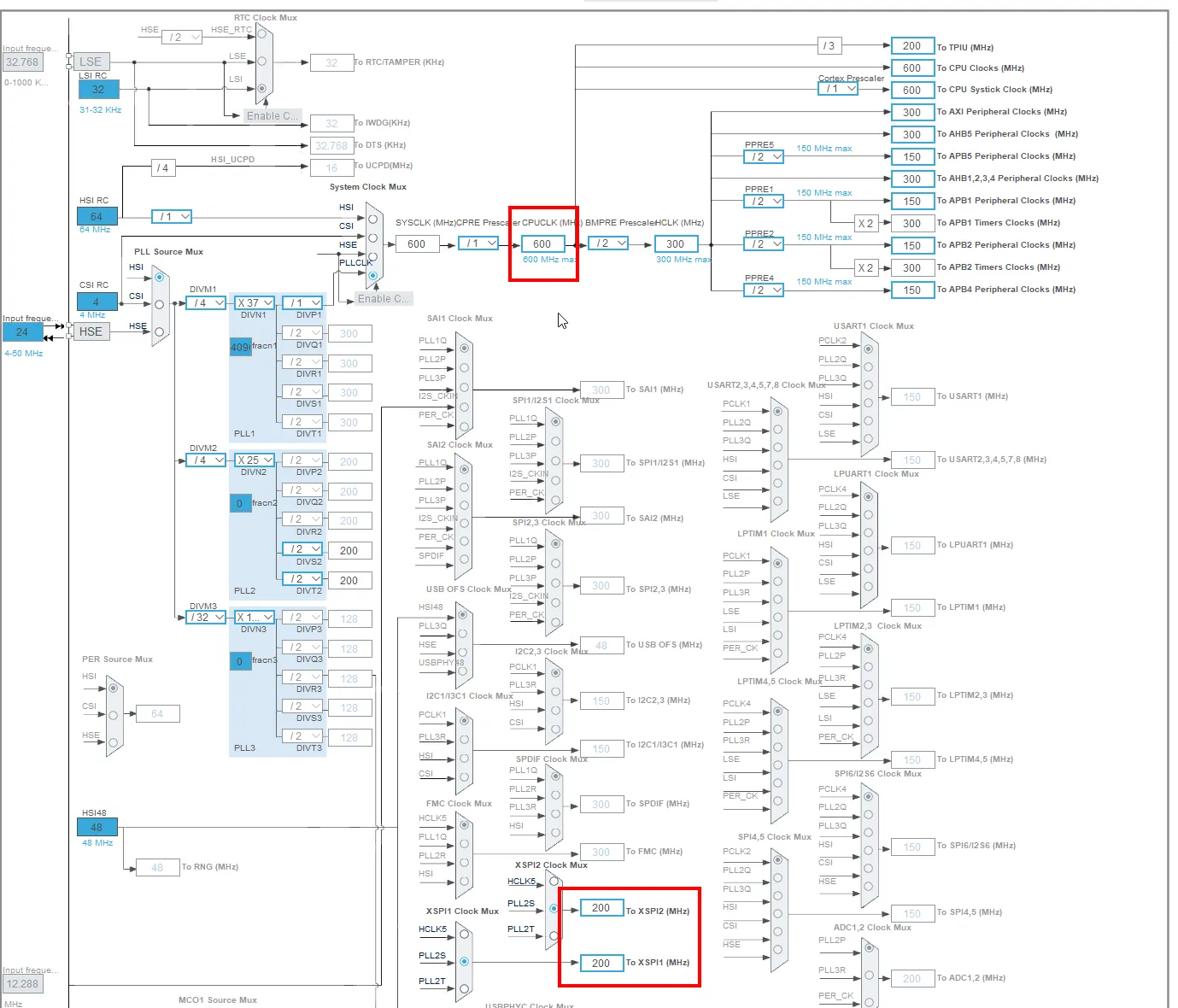
Section titled “Section 9. Clock Generation Configuration”Under the Clock Configuration tab in STM32CubeMX, we arrange the PLL (Phase-Locked Loop) multipliers and dividers to guarantee the microcontroller operates at its absolute peak frequency of 600 MHz. Simultaneously, we must verify that the branches feeding the XSPI1 and XSPI2 buses hit their exact target limit of 200 MHz for maximum memory throughput.
Section 10. GPIO Output Configuration
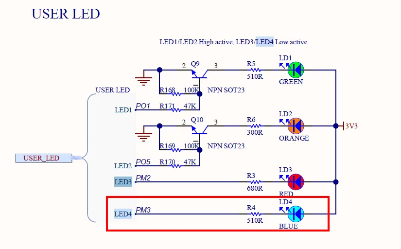
Section titled “Section 10. GPIO Output Configuration”To visually validate that our firmware is successfully executing from the external memory, we will configure a basic GPIO output. Pin A10 (hardware label PM3) is wired to the board’s blue user LED. We will allocate this pin exclusively to the Application context and set it as a standard Push-Pull output. Later, we’ll toggle this pin every 500 ms in our while(1) loop.
================================================================================GPIO CONFIGURATION - STM32CubeMX (PM3 / LED4)================================================================================
[Pinout View]  - Pin Name:                    PM3  - Pin Selected Mode:           GPIO_Output
[Configuration > GPIO Table / Parameters]  - Pin Context Assignement:     Application  - GPIO output level:           Low  - GPIO mode:                   Output Push Pull  - GPIO Pull-up/Pull-down:      No pull-up and no pull-down  - Maximum output speed:        Low  - User Label:                  LED4  - Signal on Pin:               n/a  - Peripherals:                 n/a  - Modified:                    Checked (Yes)================================================================================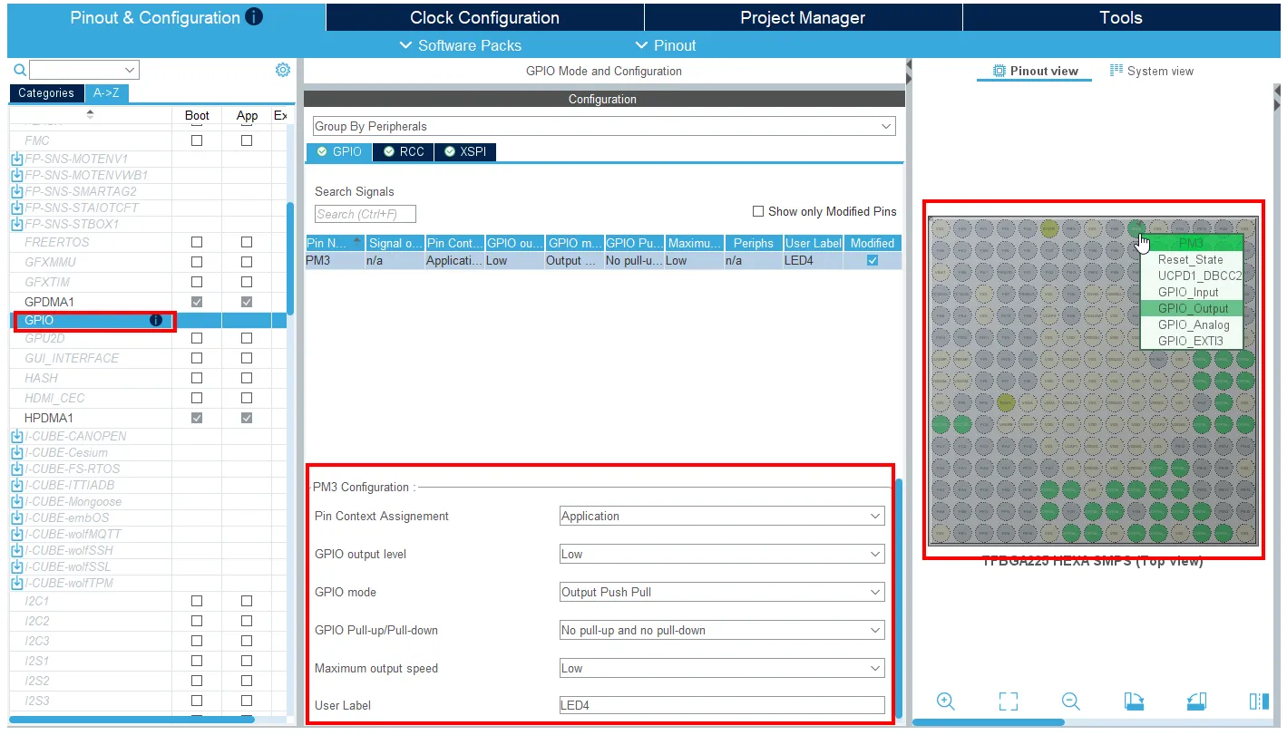
Section 11. Code Generation
Section titled “Section 11. Code Generation”With all previous hardware definitions successfully routed and parameterized:
- Navigate to the Project Manager tab.
- Under Toolchain/IDE, select STM32CubeIDE.
- Click the Generate Code button at the top right to scaffold the project structure.
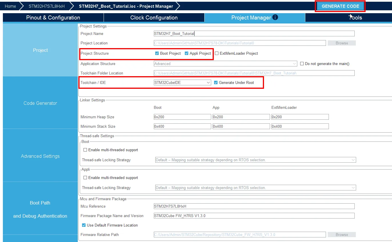
Once code generation finishes, click on the Open Project option. This will launch the STM32CubeIDE development environment directly, importing the dual-context directory structure (Boot and Application) ready for compilation.
Section 12. Testing the Code
Section titled “Section 12. Testing the Code”12.1 Bootloader Tuning and Debugging
Section titled “12.1 Bootloader Tuning and Debugging”Inside the main() function of the Boot subproject, we must add cache invalidation instructions before making the jump to external memory. This guarantees pipeline and cache coherency, ensuring the processor doesn’t fetch stale data or instructions during the transition:
/* USER CODE BEGIN 2 *//* Invalidate internal caches */SCB_InvalidateICache();SCB_InvalidateDCache();/* USER CODE END 2 */Compile the Boot project. To debug this specific code, the debugger configurations can be left at their defaults, as the compiled binary is flashed directly into the microcontroller’s small internal Flash.
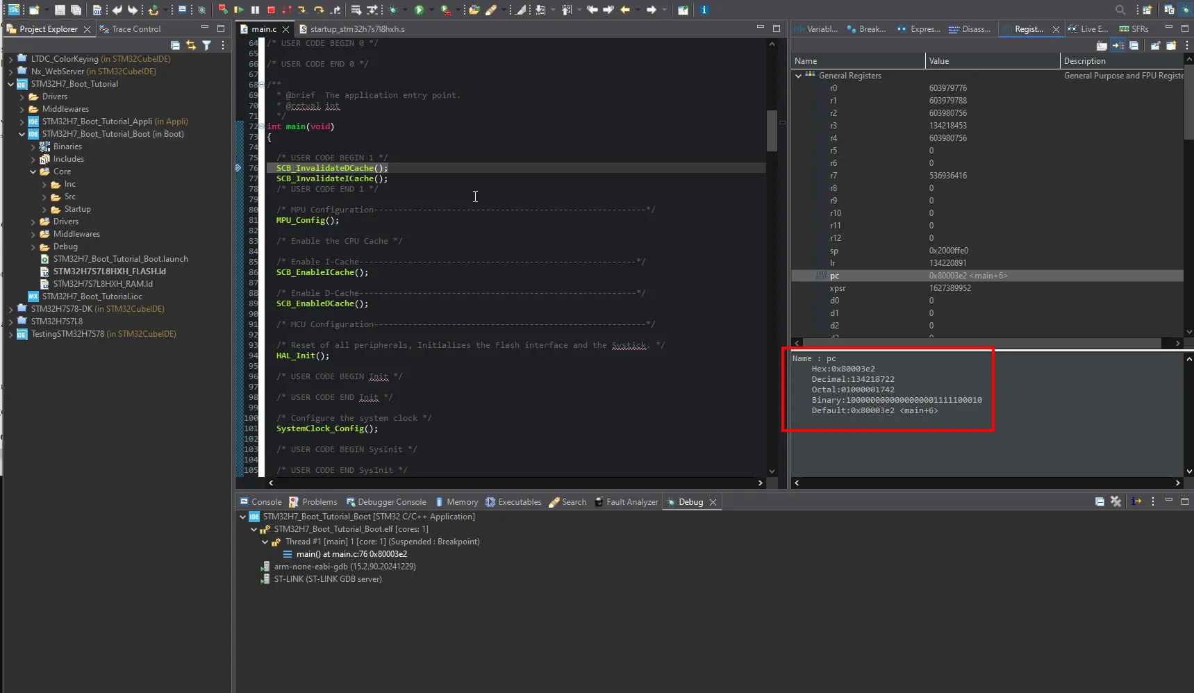
Before running the debugger, set a breakpoint at the SCB_InvalidateDCache() call. When the execution halts, inspect the Program Counter (PC). You should observe that it is in the 0x08000000 range, confirming we are executing from the internal Flash memory.
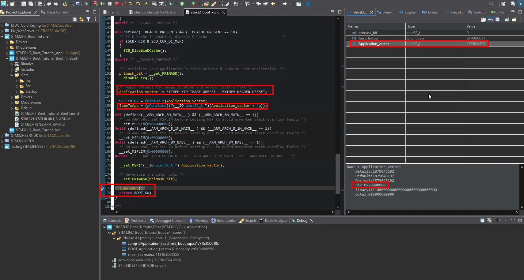
If you resume the Bootloader execution, you will reach the crucial step where the core performs the jump to the main application. This application resides in the memory range mapped to the XSPI2 peripheral (0x70000000).
12.2 Application Code and External Loader Configuration
Section titled “12.2 Application Code and External Loader Configuration”Switching to the Application project, we embed the LED4 blinking logic inside the while(1) loop in main.c:
/* USER CODE BEGIN WHILE */while (1){    /* USER CODE END WHILE */
    /* USER CODE BEGIN 3 */    HAL_GPIO_TogglePin(LED4_GPIO_Port, LED4_Pin);    HAL_Delay(500);}/* USER CODE END 3 */
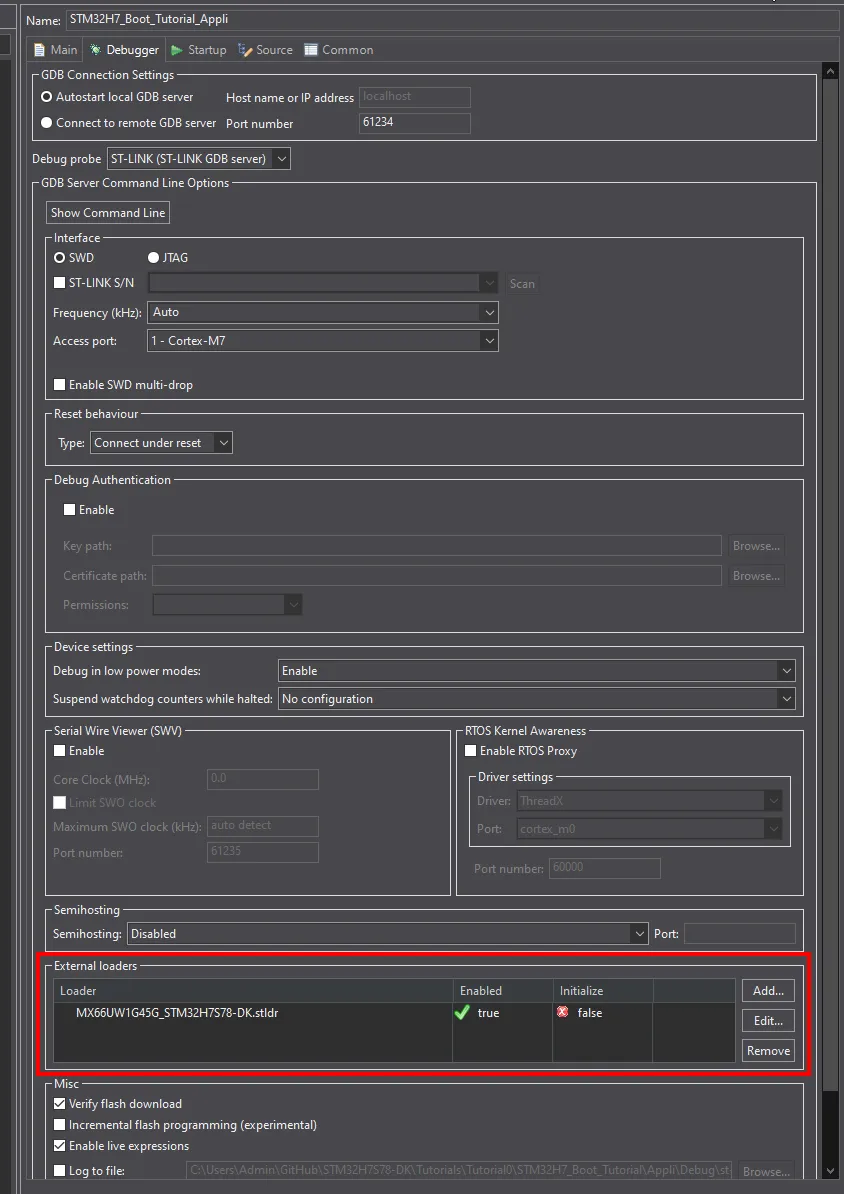
Because this application code is meant to be hosted on an external memory chip, the standard ST-LINK programmer cannot flash it natively. It requires the assistance of an External Loader—a small piece of software temporarily loaded into the MCU’s RAM to manage the flashing process for the external NOR Flash. Fortunately, ST provides pre-compiled loaders for this evaluation board.
To set this up:
- In STM32CubeIDE, open your debug settings via Run > Debug Configurations…
- Select your application under STM32 C/C++ Application.
- Switch to the Debugger tab and locate the External Loaders section at the bottom.
- Check the Enable External Loader box, click Scan, and add the loader corresponding to the Macronix Octo-SPI memory on this board.
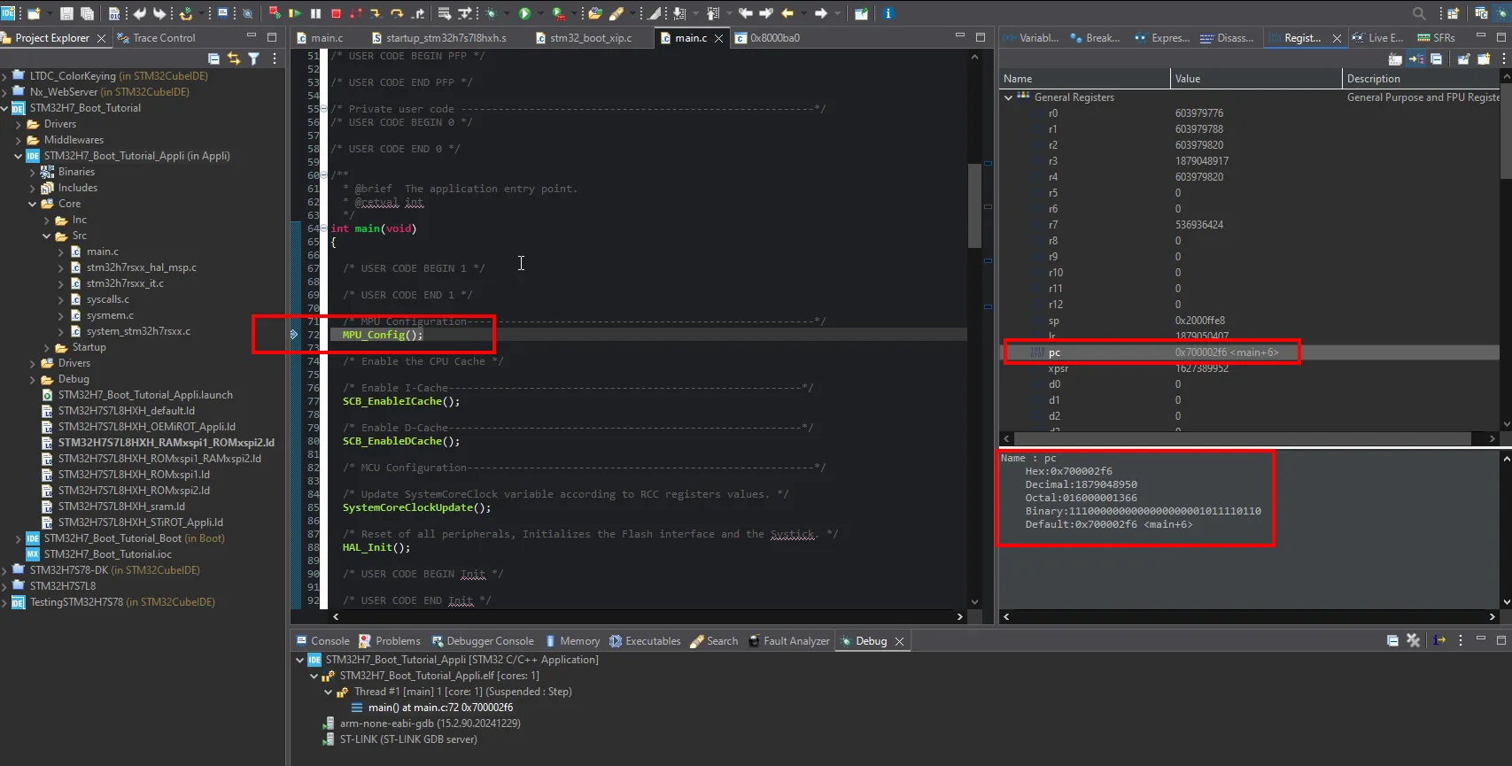
When you launch the debug session for the application and perform a “Reset the chip and restart the debug session”, the execution halts at the application’s main() function. If you check your CPU registers, the Program Counter (PC) will now reflect a value in the 0x70000000 range. This undeniably proves that your firmware is correctly executing in place (XIP) from the external XSPI2 memory!
Project Repository
Section titled “Project Repository”You can clone the complete source code, the .ioc configuration file, and the dual-project structure created in this tutorial from the official GitHub repository:
- 🔗 Repository: https://github.com/rcocoletzim/STM32H7S78-DK.git